LCD_16-2_Characters-Green_Yellow_back_light


Cautions
The LCD panel is made by glass. Any mechanical shock (eg. dropping from high place) will damage the LCD module.
Do not add excessive force on the surface of the display, which may cause the Display color change abnormally.
The polarizer on the LCD is easily get scratched. If possible, do not remove the lCD protective film until the last step of installation.
Never attempt to disassemble or rework the LCD module.
Only Clean the LCD with Isopropyl Alcohol or Ethyl Alcohol. Other solvents(eg.water) may damage the LCD.
When mounting the LCD module, make sure that it is free form twisting, warping and distortion.
Ensure to provide enough space(with cushion) between case and LCD panel to prevent external force adding on it, or it may cause damage to the LCD or degrade the display result.
Only hold the lCD module by its side. Never hold LCD module by add force on the heat seal ot TAB.
Never add force to component of the LCD module. It may cause invisible damage or degrade of the reliability.
LCD module could be easily damaged by static electricity. Be careful to maintain an optimum anti-static work environment to protect the LCD module.
When peeling off the protective film from LCD, static charge may cause abnormal display pattern. It is normal and will resume to nomal in a short while.
Take care and prevent get hurt by the LCD panel sharp edge.
Never operate the LCD module exceed the absolute maximum ratings.
Keep the signal line as short as possible to prevent noisy signal applying to LCD module.
Never apply signal to the LCD module without power supply.
IC chip(eg. TAB or COG) is sensitive to the light. Strong lighting environment could possibly cause malfunction. Light sealing structure casing is recommend.
LCD module reliability may be reduced by temperature shock.
When storing the lCD module, avoid exposure to the direct sunlight, high humidity, high temperature or low temperature. They may damage or degrade the LCD module.
Schematic
Block Diagram

Specification
LCD Display Mode: STN, Positive, Transflective
Display Color: Deep Blue/ Yellow Green
Viewing Angle: 6H
Driving Method : 1/16 duty, 1/5 bias
Back Light : Yellow-Green LED backlight
Outline Dimension: 803615.8 MAX
- Color tone may slightly change by Temperature and Driving Condition.
- The Color is defined as the inactive/background color
AC Characteristics
Vss=0V,VDD=5V,TOP=25℃
| Item | Symbol | MIN | TYP | MAX | Unit |
|---|---|---|---|---|---|
| E cycle time | tc | 1500 | - | - | ns |
| E high level width | twh | 700 | - | - | ns |
| E low level width | twl | 700 | - | - | ns |
| E rise time | tr | - | - | 18 | ns |
| E fall time | tf | - | - | 18 | ns |
| Address set-up time | tas | 5 | - | - | ns |
| Address set-up time | tasu | 210 | - | - | ns |
| Address hold time | tah | 15 | - | - | ns |
| Data set-up time | tdsw | 300 | - | - | ns |
| Data delay time | td | - | - | 480 | ns |
| Data hold time(write) | tdhw | 15 | - | - | ns |
| Data hold time(read) | tdhr | 30 | - | - | ns |
 |  |
| Host Writing Timing Diagram | Host Read Timing Diagram |
Pin definition and Rating
| Pin No | Pin Name | I/O | Descriptions |
|---|---|---|---|
| 1 | VSS | Power | Negative Power supply, Ground(0V) |
| 2 | VDD | Power | Positive power supply |
| 3 | V0 | Power | LCD contrast reference |
| 4 | RS | Input |
5 R/W Input In read mode R/W=HIGH Data read form the LCD module, data appears at DB0-DB7 and can be read by the host while, E=H and the device is being selected In write mode R/W=LOW; Data write to the LCD module, data appears at DB0-DB7 will be written into the LCD module at E=H->L and device is being selected. |
| 6 | E | Input | |
| 7 | DB0 | I/O | Data bus; Three state I/O terminal for display data or instruction data |
| .. | .. | .. | |
| 14 | DB7 | I/O | |
| 15 | CS1 | input | Chip Selection, When CS1=1(*1) Enable access to the Left Side (64column) of the LCD module |
| 16 | CS2 | Input | Chip Selection, When CS2=1(*1) Enable access to the Right Side (64column) of the LCD module |
| 17 | /RST | Input | Reset signal /RST = L, Display off display start line register becomes 0 no command or instruction data could be accepted /RST = H Normal running |
| 18 | VOUT | Output | Power Booster output for V0 |
| 19 | BLA | Power | Positive Power for LED backlight |
| 20 | BLK | Power | Negative Power for LED backlight |
Note:
Display or instruction data could write into the LCD mudule's driver/controllers individually or at the same time.
Only read display or instruction data form one of the driver/controller in the LCD module at a time, otherwise unexpected data collision may occur.
Mechanic Dimensions
Outline Dimension:98.060.013.7MAX (See attached outline Drawing for details)
Usage
Internal Registers
There are three registers in each section of LCD module. Each of them could be controlled independently.
Page(X) Address Register
X address register designates pages of the internal display data RAM. Count function is not available. The address should set by instruction.
Column(Y) Address Counter
Y address counter designates address of the internal display data RAM. It could be set by instruction and is increased by 1 automatically by read or write display data operations.
Display Start Line (Z) Register
Z address register indicates of display data RAM to LCD top line. It may be used for scrolling display pattern on the LCD.
Programming
Basic Setting
To drive the LCD module correctly and provide normally display, please use the following setting
Display start line(Z address )=0
LCD Display = on
- These setting/commands should issue to the LCD module while start up.
- See the Display Commands section for details.
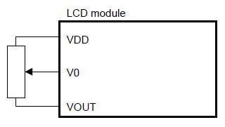
Adjusting the LCD display contrast
A Variable-Resistor must be connected to the LCD module for providing a reference to V0. Adjusting the VR will result the change of LCD display contrast. The recommended value of VR is 25k to 50k.
Resetting the LCD module
The LCD module should be initialized by setting /RST terminal at low level when turning the power on.
When /RST pull low, the LCD mudule will:
Display off
Display start line register becomes 0. (Z-address=0)
While /RST is low, no instruction can be accepted except status read. Therefore, execute other instructions after making sure that DB4=0(cleat /RST) and DB7=0(ready) by status read instruction. The conditions of power supply at initial power up are as follow:
| Item | Symbol | Min | Tpy | Max | Unit |
|---|---|---|---|---|---|
| Reset time | trs | 2.0 | - | - | us |
| Rise time | tr | - | - | 150 | ns |

Resources
Tech Support & Product Discussion
Thank you for choosing our products! We are here to provide you with different support to ensure that your experience with our products is as smooth as possible. We offer several communication channels to cater to different preferences and needs.